
Clock Card 10 based on ESP32

The ESP32 Clock Card 10 is a jitter-attenuating precision clock multiplier for applications, requiring sub 1ps jitter performance and under 0.2 ppm frequency stability. This card supports one clock input ranging from 0.1 MHz to 100 MHz and 8 non inverted and 2 inverted clock output ranging from 0.1 MHz to 100 MHz (higher frequencies possible on request).The input clock frequency and clock multiplication ratio are programmable through an I2C (ESP32-PICO-D4 USB2.0 ) interface. The clock card can be operated either from an internal TCXO or an external generator, e.g. 10 MHz from GPS receiver and is ideal for providing clock multiplication and jitter attenuation in high performance timing applications, e.g. for ADALM PLUTO SDR arrays. The card has integrated additional inputs/outputs (ESP32 peripherals) which can be controlled via WiFi or USB. These could be used, for example, for the control of mobile antenna systems, antenna switches or managing of spatial distributed arrays for MIMO applications.

Example of 24-channels clock divider

Clock Card for RTL-SDR

Clock Card is designed to generate a single clock 28.8 MHz for all receivers. The use of such an external synchronization unit has the following advantages:
- Enhanced stability;
- Reduction of the reference frequency’s 28.8 MHz phase noise;
- Improvement of the temperature characteristics;
- Opportunity to choose the required level of the frequency stability (0.1/0.5/1.0/2.0 ppm);
- Minimization of the delays and clock drift between single receivers using the star-consecutive topology

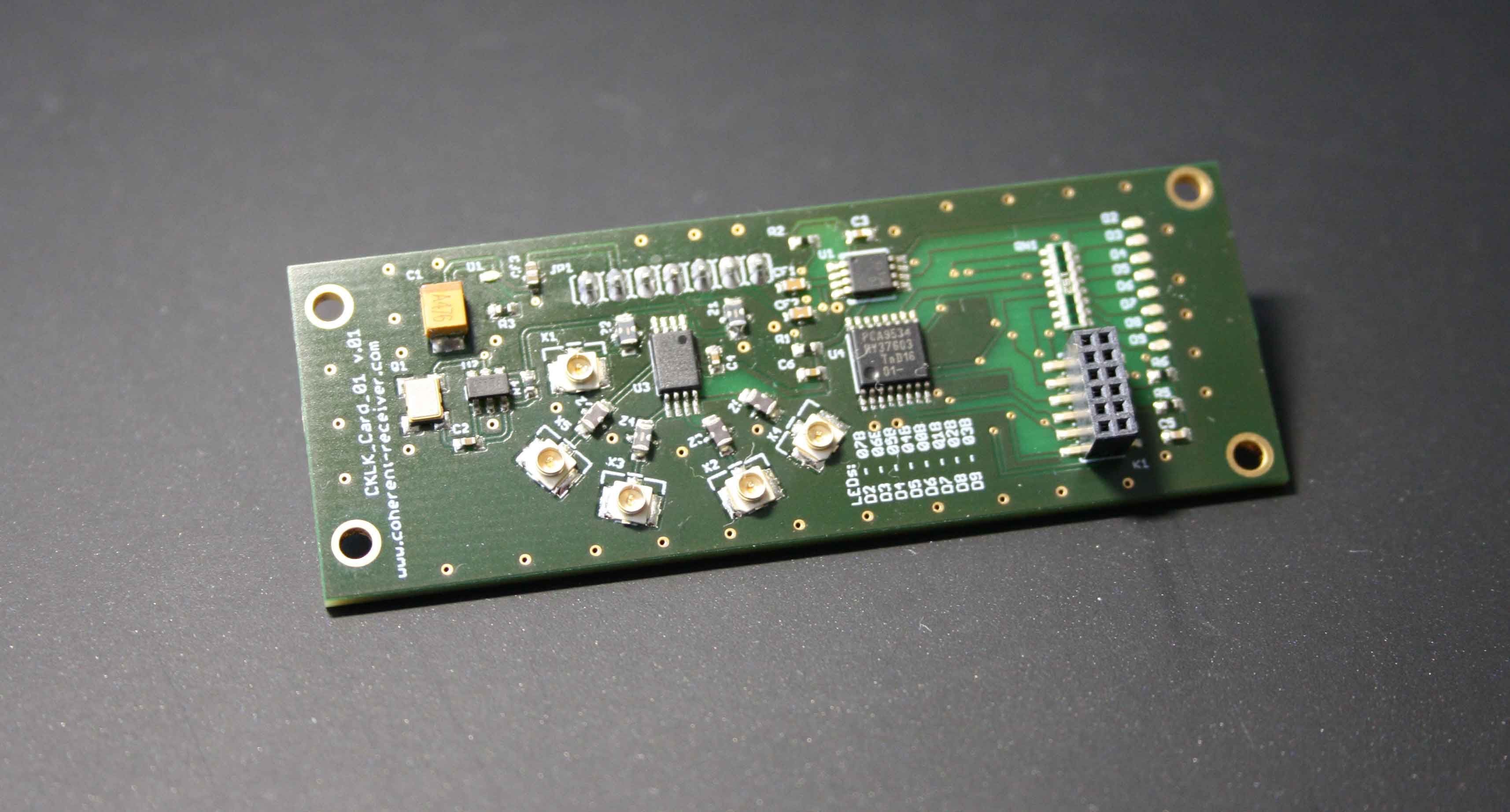
The clock card includes the following components:
- TXCO 28.8 MHz
- Default: 2 PPM initial offset, 0.5-1 PPM temperature drift.
- Optional: higher precision (0.1/0.5/1.0 ppm) is available on request.
- Buffer Gate
- Clock Buffer
- LPF (cut-off 35 MHz)
- SMD LED indicators
- I2C interface
- I2C 8bit Register
- Power indication LED (+3.3 V)
- Ultraminiature Coaxial Connectors
Buffer Gate
TCXO usually has an output resistance of about 10K , which does not allow direct connection of the TCXO to the Clock Buffer input. The Buffer Gate is necessary in order to match the high output impedance of TCXO and low 50 Om input impedance of the Clock Buffer 5PB1104. The simplest solution is to use Dual Schmitt-Trigger Inverter SN74LVC2G14. “The SN74LVC2G14 device is a high drive CMOS device that can be used for a multitude of buffer type functions where the input is slow or noisy. The device can produce 24 mA of drive current at 3.3 V, making it ideal for driving multiple outputs and good for high-speed applications up to 100 MHz” [Source: Datasheet]. The inverters are connected parallel in order to increase the output power.

Clock Buffer
The clock card is based on the high-performance LVCMOS Clock Buffer 5PB1104 produced by Integrated Devices Technology, Inc. The 5PB11xx (Datasheet) is a high-performance LVCMOS Clock Buffer Family. It has best-in-class Additive Phase Jitter of 50fsec RMS. There are five different fan-out variations, 1:2 to 1:10, available. The IDT5PB11xx also supports a synchronous glitch-free Output Enable function to eliminate any potential intermediate incorrect output clock cycles when enabling or disabling outputs. It comes in various packages and can operate from a 1.8V to 3.3V supply.
I2C 8 Bit Register
The Clock Card includes one 8-bit configuration register with LED indicators 1×8. This component enables the expansion of the underlying device (coherent receiver) with the following features:
- Input antenna switching in the direction finding system
- Management of the range filter switching in the pre-selectors
- Calibration and management of the directional antenna locations. Tuning to the necessary bearing.
- Calibration of the coherent receivers using the noise sources which enable calibration and synchronisation of data streams using the gated RF noise.
Current realization of the Clock Card integrates the PCA9534 chip that consists of an 8-bit Configuration register (Input or Output selection); 8-bit Input register, 8-bit Output register and an 8-bit Polarity Inversion register (active HIGH or
active LOW operation). The system master can enable the I/Os as either inputs or outputs by writing to the I/O configuration bits. The data for each input or output is kept in the corresponding Input or Output register. The usage of the register is described in the support section.
I2C Interface
I2C-bus repeater provides additional possibilities for the management of the peripheral devices based on the I2C-interface, e.g. low-speed DAC/ADC, step motor, sensor information reading (e.g. temperature, ventilator cooling, system control), etc.
LPF
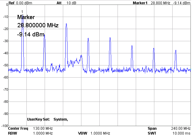
In general, the usage of the external clock buffer can lead to additional interference. Synchronization signals, which are square pulses at the 28.8 MHz, create a wide range of signals with harmonics, which are multiples of the 28.8 MHz: 2fs, 3fs, 4fs, 5fs, and can be the source of additional interferences. Therefore, it is necessary to utilise a filter with a nominal cutoff frequency at 29 … 30 MHz for the suppression of higher order harmonics (see section Low Pass Filters 30MHz Cards for more information).
| Measuring Points |
Signal Wave Form | EMI Suppression Effect |
|---|---|---|
| B | 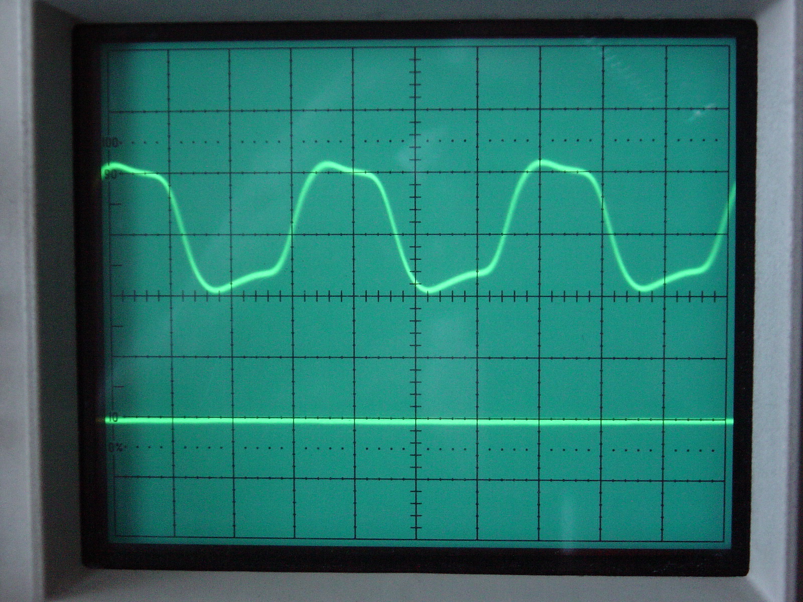 |
 |
| A, C |  |
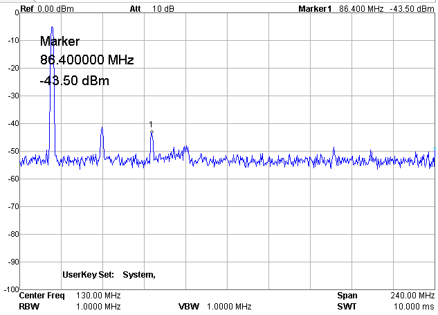 |
As seen from the table, using LPF with a cut-off frequency of 35 MHz substantially reduces the unwanted harmonics, and hence, reduces the possibility of undesired spurs in the spectrum of the received signal.
Ultraminiature Coaxial Connectors
Ultraminiature Coaxial Connectors are installed on the card in order to distribute the clock frequency on all single receivers using coaxial pigtails. The usage of coaxial pigtails reduces the phase noise and eliminates the interference of the clock frequency, including harmonics, with the received signal.
Example: 2 ppm clock
Example: 0.2 ppm clock

The clock generator and clock expansion cards are not restricted to the 28.8 MHz. Custom builds are possible for other clock frequencies with required precision.
Expansion Card for RTL-SDR
The Expansion Card has the same architecture as the Clock Card but does not include TCXO 28.8 MHz and Buffer Gate.
